The Class-A Amplifier Site
This page was last updated on 20 July 2001
15-20W Class AB Audio Amplifier
A design with class-A performance but reduced thermal dissipation
by J. L. Linsley Hood
(Wireless World, July 1970)
Many class B designs can be operated in class A at low power levels if the quiescent current is increased. However, this often worsens the distortion characteristics of the output stage, particularly at intermediate (and audibly important) power levels, by displacing the crossover point to a region where the transfer slope is much steeper, and the crossover discontinuity therefore much more prominent. This effect is considerably accentuated by the fact that almost all modern transformerless power amplifier systems use either Darlington pair or augmented (p-n-p/n-p-n) emitter follower output pair configurations, and these have a very high mutual conductance.
The use of a complementary pair of emitter followers, driven from a voltage source having an output impedance which is very much lower than the normal input impedance of the output devices, appeared from this line of thought to offer the best way of minimizing the several problems mentioned above.
In practice, the necessary low impedance base-emitter paths can be arranged quite simply by driving the output transistors from a suitably tapped emitter load resistor in a conventional emitter-follower circuit, provided that the current flow in this load circuit is adequate to deliver the necessary output drive.
Moreover, this type of circuit arrangement will also operate, in class A, as a straightforward cascaded emitter follower, as can be seen from the circuit arrangements shown in Fig. 1. In (a), the transistors Tr1 and Tr2 act as a conventional Darlington pair, with a resistive emitter load to which the output load ZL is coupled through C1. In (b), essentially the same circuit is employed, but using a complementary type of transistor as the second stage emitter follower.
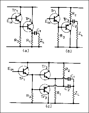
Fig. 1. Emitter follower Configurations for class A operation
It is then possible to arrange the circuit as shown in (c), so that both of these configurations are employed simultaneously. Resistors of double the ohmic value can then be employed as R1 and R2, with half the emitter current in each transistor, to give an identical matching impedance to the output load. In practice, this circuit arrangement can be simplified into the form shown in Fig. 2, and the resistors R1 and R2 deleted since the load current for each transistor can flow through the other. This also improves the efficiency since the transistors have a very high dynamic impedance and form good emitter loads for each other. The two small value resistors Rx and Ry are included to assist in stabilizing the output transistor working points.
The actual value of the quiescent current in the output stage can be set by adjustment to VR1. To avoid asymmetry, at low audio frequencies, the bypass capacitor should have as high a value as convenient.
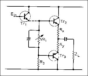
Fig. 2. Simplification of Fig. 1(c).
This arrangement of the output transistors was of particular interest to the author, since the first three stages of such an amplifier could be substantially the same as those used in the previously described class A design, of which the performance was known. In fact, the system could be constructed on the basis of the class A design, with the quiescent current reduced to a much lower level, and a pair of suitably biased back-to-back emitter followers interposed between the output and the loudspeaker load. However, this would not have made the most of such a system. In particular, it will be noted that if the potential at the emitter (or base) of Tr1 in Fig. 2 is held constant, the current through the resistor chain R3, VR1 will be constant for any particular value of VR1 and therefore the turn-on potential applied between the bases of Tr2 and Tr3 will also remain constant (or virtually so). This allows the standing current of the output transistors to be defined precisely, since the d.c. output potential can be controlled by the use of unity gain d.c. negative feedback, and this effectively controls the emitter potential of Tr3
.
Also, since the last voltage amplifier stage is not required to deliver significant power, it can be optimised for voltage gain, with an increase in the available negative feedback. A practical amplifier circuit of this type is shown in Fig. 3.
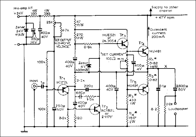
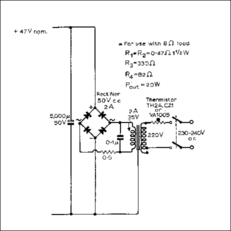
Fig. 3. Power amplifier circuit. The dotted components (680pF, 1.5kohm)
can be added if electrostatic speakers are used
The first two transistor voltage amplifier stages of this follow conventional design practice, with the collector load resistor of Tr2 boot-strapped to obtain large voltage swing at the base of Tr3 with as little second harmonic distortion as practicable. The collector of Tr3 is also partially boot-strapped in order to reduce the peak voltage swing, and improve the symmetry of the output waveform prior to the application of the loop negative feedback. (Without overall n.f.b. the distortion at full output power is a little less than 4%, almost entirely second harmonic. This is similar to the performance of a good triode valve output stage prior to the application of n.f.b.) The lower end of R3 is also fed with the output signal to improve the output voltage swing obtainable from Tr5.
The 390pF capacitor between the emitter of Tr1 and the collector of Tr2, and the 8.2ohm resistor in series with the 0.1uF capacitor across the output, provide the necessary phase-angle correction and define the high-frequency gain of the feedback loop. With the values shown there is a 6 dB/octave roll off beyond 100kHz, and the system is completely stable under all load conditions. However, with the use of a large value capacitive load there will be some overshoot on a rapid transient. The author believes that it is desirable for tonal purity, for such overshoots to be eliminated, and it is recommended, therefore, that the 390pF capacitor be shunted with a 680pF 1.5kohm combination where it is intended to drive electrostatic speaker systems. However, on normal loads this merely reduces the h.f. roll-off point, and the power output available in the 30-50kHz region, and can well be omitted.
The 100ohm wire-wound potentiometer between the bases of Tr4 and Tr5 is used to set the quiescent current level to about 200mA. The chosen current level determines the power level at which the system changes from class A to class B operation. With the suggested level of 200mA, this transfer will occur at approximately 1.2 W with a 15ohm speaker (640mW for 8ohm).
If the standing current through the output stage is increased, progressively larger output power levels can be obtained within the class A region, up to the level at which the amplifier acts as a pure class A system. The only observed penalty for this exercise is that the power supply demand and the thermal dissipation in the output transistors are both proportionately increased. However, if the output transistors are of dissimilar origin or are otherwise badly paired the operation of the circuit in class A will ensure that the distortion levels and other performance standards are attained in spite of this.
Performance characteristics
The specifications given below were obtained using the power supply system shown in Fig. 3. The amplifier was specifically designed to work from a poorly smoothed h.t. line, the values and positions of the h.t. decoupling and 'bootstrap' capacitors being chosen to avoid the intrusion of ripple into the signal circuits. The only significant difference observed in using a good quality stabilised and smoothed power supply is a small improvement in the already extremely good hum and noise levels.
Power output. 15W into 15 ohm, or 18W into 8ohm (20W with modified output circuit components values).
Bandwidth. 10Hz-l00kHz +/- 0.5dB at 2V output. 20Hz-50kHz +/- 0.5dB at maximum power output.
Output impedance. 0.03ohm (at 1kHz).
Total harmonic distortion. 0.02% at 15W/15ohm or 18W/8ohm; less than 0.02% at all power levels less than maximum output.
Intermodulation distortion. Less than 0.1%. l0W (12.3Vr.m.s.) l5 ohm, 70Hz. 1V r.m.s. 7kHz (or 10kHz).
Square-wave transfer distortion. Less than 0.2W at 10kHz.
Rise time. 3us.
Input impedance. 20kohm (approx.).
Gain. 18x.
Hum level. (Simple power supply) -70dB w.r.t. 1W.
Noise level. (Simple power supply) -80dB w.r.t. 1W. (These figures are, respectively, better than -80dB, and -85dB with the regulated power supply).
Feedback factor. 46dB (typical).
Input voltage for max. output. 850mV r.m.s.
Load stability. Unconditional.
For the perfectionist, a suitable design for a regulated d.c. power supply, with re-entrant short-circuit and overload protection is shown in Fig. 10. This gives approximately 10dB improvement in the hum and (r.m.s.-weighted) very low frequency noise.
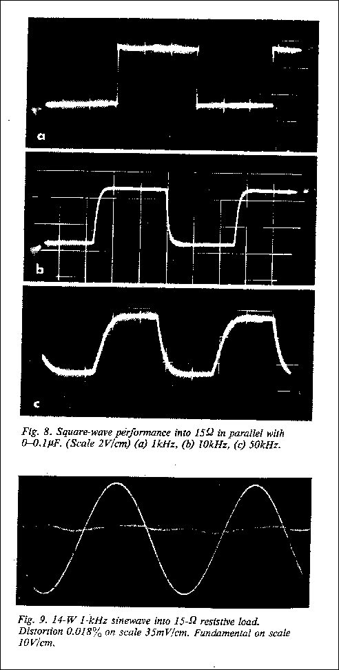
The gain/frequency, and power output/frequency graphs are shown in Figs. 4 and 5, and the relationship between output power and distortion, and signal frequency and distortion are shown in Figs. 6 and 7. The square wave performance into a 15ohm resistive load, with any value of shunt capacitance up to 0.1uF, at 1kHz, 10kHz, and 50kHz are shown in Fig. 8. The sine wave output at 1kHz, and 15W with a 15ohm resistive load (42.5Vp-p) and the associated harmonic distortion (representing 0.02%) is shown in Fig. 9.
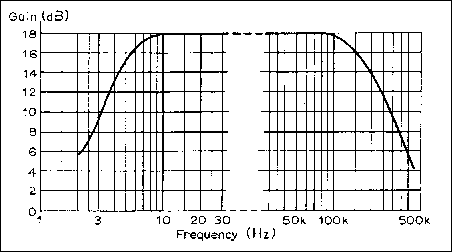
Fig. 4. Gain/frequency characteristics.
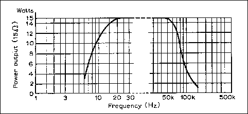
Fig. 5. Power output/frequency characteristics.
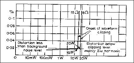
Fig. 6. Power output/distortion characteristics. The 8ohm load characteristic
was measured using the modified output-stage components.
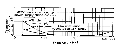
Fig. 7. Influence of signal frequency on distortion (1W into 15ohm).
Listening trials
As described last month, a number of experiments were done during the development of this circuit to try to relate audible effects to the phenomena observable and measurable in the laboratory, and a transfer distortion analyser (British patent application No.7925/1970) was made to judge the performance with non-sinusoidal waveforms. (A point was reached in the earlier stages of the design where the author's ear was no longer able to detect the subsequent improvements.)
The transient response of the 10-watt class A design (as originally published(1), without the modifications(2), suggested in October 1969 to reduce the h.f. bandwidth) is superior to that of the present circuit in the range 50kHz-2Mhz under load conditions of fairly low capacitive reactance. Under more adverse load conditions the present design will be (technically) better. However, the most careful comparative listening trials, with several of the author's long-suffering friends, have failed to uncover any audible difference between these two designs, both of which will almost certainly surpass in performance the best available valve-operated, transformer-coupled units.
Constructional points
The layout used in one of the prototypes of this design is shown in Fig. 11, using a 0.15in. matrix copper strip board. The layout should not be particularly critical provided that normal precautions are observed, such as keeping the output and input circuits reasonably well separated, and making sure that the power supply leads, and the loudspeaker return lead, connect to the board at a point close to that to which the collector leads of the output transistors are soldered.
Since the circuit has unity gain at d.c. the occurrence of a switch-on 'plop' in the loudspeaker can be avoided by the use of a suitably long time-constant in the decoupling circuit which provides the base bias for Tr1. The voltage at 'X' (Fig. 3) will then follow the base potential of Tr1 as it slowly rises following switch on. It is undesirable to have the full h.t. voltage applied during this period, and this is avoided by the incorporation of a thermistor (Radiospares TH2A or equivalent) in the mains transformer primary circuit. Since this will cause a drop of some 10-15V, this should be allowed for in the tapping point on the mains transformer. Also, since the thermistor becomes quite hot under operating conditions (this is necessary) it is important to mount it in such a way that this does not damage associated components or wiring.
The dissipation of the output transistors is normally about 8W, and the output pair can both be mounted on a single 3.5in. x 4in. black anodised, ribbed heat sink. The heat sink should be earthed - very simply by omitting the mica washer on the MJ491.
The driver transistor dissipation is of the order of 2W in some circumstances, and this is somewhat in excess of the power which can be handled safely by the normal TO-5 cased device, such as the 2N1613, unless very careful heat sinking arrangements are employed. The use of such devices as the 2N3054 or the Motorola MJE521, mounted on a small piece of black-painted aluminium sheet, say 1in. x 1.5in., gives a very large safety margin in this stage. The performance of the Motorola MJE52 1 is slightly to be preferred, and was used in all the prototypes. This stage, however, is not a very critical one, and these transistor type variations are unlikely to make a significant difference to the system's overall performance.
The Texas BC212L and 182L are the preferred transistor types for Tr1 and Tr2, although the 2N1613 was also used in some development models as Tr2 with identical results. The Motorola 2N3906 and 3904 could also be used in the Tr1, Tr2 positions with almost equivalent performance, but this has not been tried. The use of 0.5W carbon film 5% resistors is suggested except in the points where higher wattages are required. R1 and R2 should be of small diameter or low inductance. The various electrolytic capacitors can be of higher value or voltage working without ill effect.
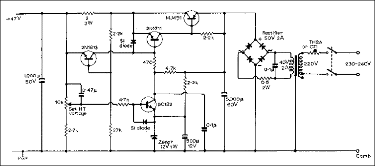
Fig. 10. Stabilised power supply with re-entrant short-circuit protection (12-49V).
Appendix 1
Calculation of power output levels obtainable with given quiescent current in class A operation.
The maximum output power which can be obtained from a power output stage such as that in Fig. 3, in class A, is entirely determined by the quiescent current and the load impedance provided that adequate h.t. voltage is available. At frequencies which are low enough for the 'wattless" components of the load current to be ignored, the maximum current excursion which can be caused to flow through the load without taking one or other of the output transistors beyond cut-off is equal to twice the quiescent current through the output stage. Since this is the 'peak' current through the load, if the waveform is sinusoidal, the r.m.s. equivalent current will be 2 x Iq / √2, and at low frequencies, the power developed in the load will be 2 x Iq^2 x RL.
For example, if the stage is required to operate in class A up to one watt, with a 15 ohm load, the peak current swing through the load must be 1 = 2 x Iq^2 x 15, or Iq = l83mA. Similarly, for an 8ohm load, Iq = 250mA.
With the standing current suggested (200mA), 1.2 watts or 640mW will be given for 15ohm and 8ohm loads respectively. This should be adequate for most normal listening. For full class A operation up to 15W, quiescent currents of 710mA and 970mA respectively will be required.
Appendix 2
Output transistor protection
The use of class B output circuit configuration (and class AB comes within this category at the power levels concerned) in transistor power amplifiers of this general type leads to the possibility that very high instantaneous currents can flow, which will lead, regrettably, to the equally instantaneous destruction of the transistors involved, if the amplifier is operated at maximum drive into an effective short circuit, and this could be a load with a very high capacitive reactance, in some cases.
The classic system for output transistor protection, using two input bypass transistors, is that due to Bailey(3), and this is also applicable to the output circuit of this design. However, because of the d.c. asymmetry between the potential at the base of Tr3 and the output point 'X', a much simpler arrangement can be used, consisting solely of a good quality (low leakage) zener diode between these two points, with the positive zener end connected to the base of Tr3. Any 4 - 4.7V zener will do provided that the leakage current at 3V reverse, and 0.4V forward, is less than 10uA. The ITT400mW series ZF4.7 is quite suitable. Again, for 20W output into 8ohm, the resistors R1 and R2 must be reduced to 0.47ohm.
REFERENCES
1. J. L. Linsley Hood, "Simple Class-A Amplifier", Wireless World, April 1969.
2. "Letters to the Editor", Wireless World, October 1969.
3. A. R. Bailey, "Output Transistor Protection in A.F. Amplifiers", Wireless World, June 1968.
HISTORY: Page created 20/07/2001