The Class-A Amplifier Site
This page was last updated on 12 January 2002
15-20W Class AB Audio Amplifier
Letters to the Editor of Wireless World
Class AB amplifier (August 1970)
Mr. Linsley Hood is quite correct when he states that the operation of transistor output stages in class AB can cause increased distortion, because of the change in the slope of the transfer characteristic around the crossover point. However, I fear that he is wrong in supposing that a low source impedance overcomes the problem.
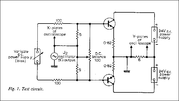
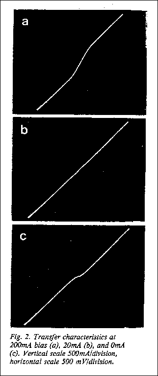
Fig. 1 shows a test circuit which I constructed to measure the transfer characteristic of the output stage under various bias conditions and the results are shown in Fig. 2 for 200mA, 20mA and 0mA. Note the prominent change in slope at 200mA bias. In the test circuit the transistors are operated in the common emitter mode to enable the changes in the slope of the transfer characteristic to be seen more easily, but this does not alter the validity of the results since the effect of putting the load into the emitter circuit is only to provide local negative feedback. Under the same conditions a push-pull emitter follower using an output stage with the transfer characteristic of Fig. 2(b) will produce less distortion than a similar output stage with the transfer characteristic of Fig. 2(c).
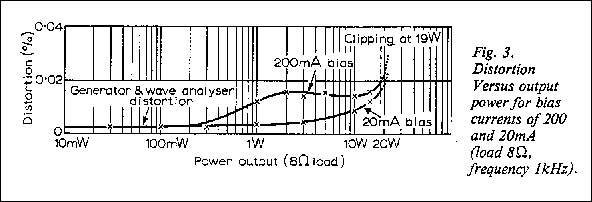
To check this I constructed Mr. Linsley Hood's amplifier and measured the distortion at 200mA and 20mA bias current with a Marconi TF2330 wave analyser and TF2100/1M1 low distortion oscillator. The results are shown in Fig. 3 and show clearly the improvement in distortion at intermediate output levels produced by the lower bias current. However, in spite of the excellent results obtained I would not advise constructors of this amplifier to use a bias current as low as 20mA as it tends to be rather unstable. A bias of 50mA would be about the optimum and at this level there would still be a "hump" in the distortion curve but it would be smaller than at 200mA bias and removed to a lower power level. I would also consider the use of a temperature compensating diode or transistor in the bias network strongly advisable, to minimize thermal variations.
Mr. Linsley Hood is also incorrect when he states that the emitter follower driver Tr3 presents the output transistors with a low source impedance. This would be true if it were not for the bootstrap capacitor which raises the effective value of the 6.8kohm load resistor in Tr2 collector to around 5Okohm. Thus the source impedance seen by the output transistors is about 1kohm, i.e. about twice their input impedance with an 8ohm emitter load.
A further point concerns the current gain of the output transistors. The specified gain spread for the MJ481/MJ491 devices used is 30-200 at 1A. As only 40mA is available from the driver stage the peak collector current with minimum gain devices is only l.2A. This corresponds to an output power of about 8 watts into 15ohm and 5 watts into 8ohm. To achieve the output power claimed by the author the output transistors need to have a minimum current gain of around 80 at 1A. Perhaps the author could suggest alternative component values for those unfortunate enough to get low-gain transistors.
One last point. The author obviously attaches great importance to "square wave transfer distortion" but he has not yet told us how he defines it. It is well known that any network, whether it be active or passive, that does not have a linear phase/ frequency characteristic will produce transient distortion of a square wave. Does the author consider that, for example, an L-C filter with a sharp cut-off at 50kHz would produce audible distortion? The ringing produced by such a filter would be very similar to that produced by an audio amplifier with a load of 15ohm and 2uF.
D. S. GIBBS,
Bury, Lancs.
The author replies:
Mr. Gibbs' letter raises a number of interesting points, with some of which I concur. However, I regret that he has misunderstood the argument in some cases.
To take his points separately.
1. Optimum quiescent current: The fact that there is an optimum value of quiescent current in a class B output stage for minimum harmonic distortion is well known and is not in dispute. This optimum current depends, among other things, on the current gain of the output transistors (or the product of the current gains if a Darlington pair or a similar output stage configuration is used) and, to a first approximation, the higher the effective current gain of the individual halves of the output stage the lower the optimum value of quiescent current. From the figures Mr. Gibbs quotes it would seem that the transistors he chose for this experiment had a high value of current gain.
However, this is not the point. I believe that the bulk of normal listening is done with output power levels which are of the order of only 50-250mW, only the very occasional transients demanding power levels in the 1-2 watt region. I also believe that it is advantageous for the amplifier to operate in true class A bias conditions for normal listening power levels, in that this avoids most of the ill-effects which can arise in class B, for example due to mismatched output transistor characteristics. These ill-effects produce the bulk of the high order harmonic and intermodulation distortions which appear to be objectionable to the ear.
Therefore, the question is simply which output stage configuration will operate best overall, with a forward bias of say, 200mA (this being chosen to allow class A operation up to 600mW-1.2 watts with 8-15 ohm loads). The simple complementary emitter follower combination appears to be the best one for this purpose.
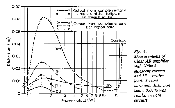
The measurement of very low order harmonic distortion levels is difficult, and is influenced by such things as h.t. supply impedances, lead connections, etc. and I am grateful therefore to find that Mr. Gibbs' measurements confirm my own findings that such a design, with such an output stage and forward bias does not give rise to harmonic distortion levels in excess of 0.02%. My own subsequent measurements with a harmonic analyser show that the distortion produced in the 'hump' region is mainly 3rd harmonic, whereas the higher magnitude of distortion produced by a more conventional complementary Darlington pair biased to 200mA, in a similar circuit, also contains more of these audibly objectionable higher order harmonics (see my Fig. A). Whether one has 0.015% or 0.005% t.h.d. is probably only of academic interest to the user.
2. Base-emitter impedance: For good high-frequency and transient performance it is desirable, I believe, that the impedance between base and emitter of the output transistors should be low. In the case of the class AB amplifier circuit, this condition is met by the 100ohm potentiometer, 400uF combination connected between the bases of the two output stage transistors, since when one of these is cut-off the other is conducting and provides the necessary base-to-emitter return path. The use of a relatively high driver impedance is actually advantageous in minimizing harmonic distortion due to the transistor base impedance non-linearity.
3. Output power: The question of the range of current gains to be found with the M481-491 series transistors has been raised before in different contexts in these columns. My own experience with quite a large number of these is that the lowest current gain encountered, at 1A, is of the order of 75, and most, in fact, lie in the 100-150 bracket. However, this is not really an important limitation under dynamic conditions, because the effect of the bootstrap connection to the emitter load of Tr3 allows adequate drive current even with low-gain transistors.
4. Audible effects of transient overshoots on reactive loads: My experimental findings are that there is an occasional audible difference between an amplifier whose stability under reactive load conditions is such that no overshoots are produced with a transient input and one which 'rings'. I do not think that this has anything to do with the nature of the h.f. response curve although it is evident that a 'ring' can be produced by a steep-cut low-pass filter. In the case of an audio amplifier driving a loudspeaker load, my own hypothesis is that some loudspeaker systems, under some dynamic conditions, can provide a negative reactive impedance, and this, however transitory, can exaggerate incipient reactive load instabilities present in the amplifier, and introduce spurious (and audible) waveform distortions.
I will take this opportunity of adding a personal note. In the original draft of my article, I walked into a philosophical booby-trap on the output power calculations, through overlooking the fact that current can flow both ways through the load. On subsequent consideration I became aware of this error, and the calculations shown in the Appendix 1 are correct. That part of the article relating to this - the last half of the third paragraph on page 322 - is however, in error. The values 1.2W and 640mW should be substituted for the 300 and 160mW figures shown and the remaining 35 words of that paragraph deleted. I apologize to readers for this contradiction appearing in the text.
J. LINSLEY HOOD.
Class AB - some questions (September 1970)
Following the two articles on a class AB amplifier design by Mr. Linsley Hood and also the correspondence in the August issue, we would like to raise several points concerning the specification.
Total harmonic distortion is specified as less than 0.02% at all power levels below maximum output, but this is presumably (see Figs. 6 and 7) only at 1kHz though not specified as such. What are the distortion levels at 100Hz and 10kHz at full output, for example?
When quoting a noise level for the amplifier, the noise bandwidth of the measurement was unspecified thus rendering the result as meaningless as quoting a frequency response without limits (e.g. +/- 3dB).
A value for "square-wave transfer distortion" is given as 0.2% at 10kHz but the power level is not specified. As "square-wave transfer distortion" is a non-standard quantitative measurement, for the result to be meaningful, an explanation is required as pointed out by Mr. Gibbs in his letter in the August issue. Also results for other amplifiers, for example a good class B amplifier, would be useful for comparison.
MARTIN SMITH and H.P. WALKER,
Southampton, Hants.
Notwithstanding the perfection of Mr. Linsley Hood's latest amplifier in practice, I would differ with him over some of the points he raises in the July issue.
A Darlington pair has a lower mutual conductance than the output transistor on its own. The converse can only be true of the complementary pair configuration. His first paragraph attributes a higher value to both pairs.
The overall linearity of the output stage of his Fig. 2, when driven from a genuinely low source impedance, does depend on the quiescent current contrary to his expectations. A high drive impedance is the answer, with a low inter-base impedance. This does not impair the cut-off performance as the conducting transistor presents a low base-emitter impedance to the one being cut off.
The output stage of Fig. 3 operates between the common emitter and the common collector modes. The true emitter follower of Fig. 2 has an inherent distortion of about 100 times less than Fig. 3, provided that the source impedance is low enough and the quiescent current is appropriate. Infinite values of bootstrap capacitance are necessary to secure pure common emitter operation; this circuit is predominantly common emitter above 30Hz. His calculation of class A output power assumes that the output transistors have a constant mutual conductance. Due to the bend in this characteristic at low collector currents they do not cut off as soon as expected. The class A output of either version is nearly 2 amps pk-pk. Using a standing current of 100 mA and no emitter resistors, a class A output of over 5 amps pk-pk is available. (The traditional definition of class A does not preclude current ratios between the two halves of 10^8.)
A high class A power is not, ipso facto, a particular virtue. The correct quiescent current is related to the linearity of the output stage under dynamic conditions, and this ought to be significantly lower than that required by full class A operation, in a good class AB design.
The mutual conductance of MJ 481/491 with 0.82ohm emitter resistors is 1mho at high currents; this falls to 0.5mho at a collector current of around 20mA. If Tr3, 4, 5 have high current gains, so that the drive impedance really is low, this is the optimum quiescent current with a bandwidth of a few kHz. Higher quiescent currents worsen the performance. A current of 200mA is undoubtedly right for bandwidths greater than this, but no compromise would be necessary if the drive impedance was high enough for all combinations of transistors.
Poor matching of the output transistors is extremely unlikely to cause any noticeable deterioration of the performance, except to a distortion meter; low gains may even be advantageous in certain cases. Full class A operation is unnecessary in both these circumstances.
My final point concerns the avoidance of temperature-compensation in the biasing of the output stage. The penalty for this is very poor thermal stability in the 8ohm version.
D. L. D. MITCHELL,
University of Bradford.
Class AB amplifiers (October 1970)
I am grateful to Mr. Mitchell for his letter in the September issue concerning my class AB amplifier, but there are some points which he makes which, I feel, should not pass without challenge.
In particular he states that a Darlington pair output stage has a lower mutual conductance than the output transistor on its own. While, in theory, this could follow from the fact that the second transistor imposes an impedance in the emitter circuit of the first, this situation does not arise under any but near zero source impedance systems, as I have illustrated in the transfer characteristic graphs on the next page.
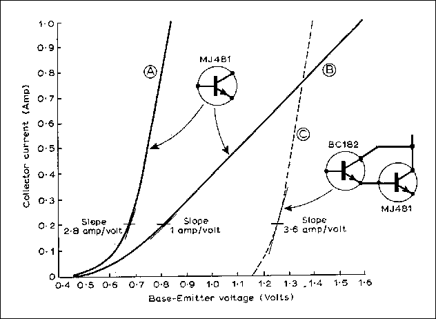
Curve A is the transfer characteristic of a simple (MJ481) transistor with a source (base input circuit) resistance of 10 ohms. Curve B shows the performance of the arrangement but with a source resistance of 100 ohms. Curve C is that of the same output transistor, but with an input Darlington configuration using a BC182 input transistor. There is no measurable difference in performance, in this configuration, with source resistances of 10, 100 or 1,000 ohms.
In the event, the slope of the Darlington pair, at 200mA, which was my chosen quiescent current, is 3.6 amps/volt as compared with 2.8 amps/volt for the simple output transistor.
The presence of as little as 100 ohms input circuit resistance reduces this to 1 A/V, which confirms the point I made in my article, which was concerned, implicitly, with the circumstances which would exist in a practical design.
The second point on which I differ from Mr. Mitchell concerns the conditions of operation of a class A stage. I believe this classification should be restricted to systems in which each component of the output stage operates in its linear region over the whole of its effective output swing. The mere fact that one or other of the output transistors is not completely cut off is not enough to satisfy this requirement.
Although I had not mentioned this point specifically in the article, the use of the amplifier in true class A does bring about a reduction in the distortion typically to below some 0.01%, at power levels below 15 watts, over the frequency range 100Hz-5kHz, and the distortion content then decreases linearly with reduction in output signal magnitude.
My decision, in the design of the amplifier, to employ a variable resistor, as a source of bias, between the bases of the output transistors, rather than a more complex temperature compensation network was based partly on the convenience of adjustment of such a biasing system, as compared with, say, a string of diodes (two forward biased silicon diodes will, in fact, give almost the correct quiescent current, and this arrangement was used in some of the prototypes in use by friends) and partly on its lesser proneness to catastrophic failure than transistor "amplified diode" systems.
My curve B indicates the relative insensitivity of the single transistor output stage to variations in forward bias (and the choice of 200mA quiescent current very much reduces thermal effects, even with an 8 ohm load!) as well as the excellent transfer linearity of such a system which contributes to the lower harmonic distortion figures obtainable with such an output stage in comparison with the more normal push-pull configurations.
Both Mr. Mitchell and Mr. Gibbs (letters, Aug.1970) have taken me to task for my observation in the article that "the use of a complementary pair of emitter followers 'driven from a low source impedance' appeared to offer the best way of minimizing the several problems" described in the introduction.
The article in question was in fact written as one, rather lengthy, article which was divided in two for convenience of publication, and this division, coupled with some editorial deletions, resulted in the observation above being given an unexpected degree of prominence. Since I was, at this stage, reviewing the thought processes which had led to the choice of this output stage configuration, it would have been better if I had continued "and this type of stage was therefore chosen as the starting point for this design".
In the event, both the preliminary calculations and the initial experiments indicated that it was neither practicable nor desirable, from the point of view of linearity of operation, that the output stage should have a low source impedance and the solution suggested by Mr. Mitchell in his letter, that of a relatively high driver impedance with a low inter-base impedance, was the configuration which had been adopted in the final design.
In reply to the letter from Messrs Smith and Walker in the September issue I would point out that the total harmonic distortion was quoted at 1000 Hz, because this is the recommendation of the B.S. and DIN specifications. The t.h.d. figures, at full output, at 100Hz and 10kHz, are typically 0.04% and 0.06% respectively. At low frequencies the harmonic distortion is mainly influenced by the impedances of the power supply bypass capacitor and the decoupling and 'bootstrap' capacitors, and an improvement can be made, if necessary, by increasing the value of these.
At high frequencies, the distortion content is mainly determined by the deliberate and necessary reduction in the open-loop gain, and feedback factor, required to maintain good reactive load stability, although the circuit layout and stray capacitances have some effect.
I apologise for the omission of the bandwidth limits for the noise figure measurements. These were effectively those imposed by the amplifier gain/frequency characteristics, as would be measured by a very wide bandwidth millivoltmeter. The use of a more restricted bandwidth, say 20Hz-20kHz, would allow an apparent improvement in the specified noise figure. (It is, in fact, quite inaudible.) However, on looking through back numbers of Wireless World I find that other authors have been equally remiss in omitting measurement bandwidths when quoting noise levels. This point will, perhaps, be noted in the future.
I regret that the measurement parameter "square wave transfer distortion" was not accompanied by some further explanation. In practise, transfer distortion is measured by comparing electrically the waveforms at the input and output of the system under test, and then expressing the error arising in the transfer as a percentage of the input waveform, as measured on an r.m.s. calibrated voltmeter such as that used for conventional t.h.d. measurements. Any convenient waveform may be used for this purpose.
Typical values for transfer distortion with conventional audio amplifier designs using a 10kHz square wave and a resistive load range from 0.2% to 10%. Square-wave transfer errors as high as 30% are fairly common under reactive load conditions, and this, in conjunction with the relatively high distortion levels sometimes found at low volume levels, may account for much of the so-called 'transistor sound'. Unlike harmonic distortion, transfer distortion with reactive loads may worsen as the amount of negative feedback is increased.
J. L. LINSLEY HOOD,
Taunton, Somerset.
Class AB amplifiers again (December 1970)
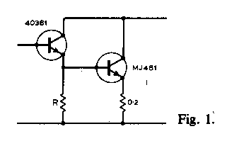
Mr. Linsley Hood's reply in the October issue to my letter (August) does indeed clear up the difficulties I experienced in following his article and his reply to Mr. Gibbs (August issue), but I feel bound to justify my objections more fully. I understand the mutual conductance of a transistor or a pair of transistors to be dIc/dVbe. Vbe is measured between the input base and output emitter, under precisely those near zero source impedance conditions to which he refers. With values of less than an ohm the shape of the basic mutual characteristic of the MJ481 is preserved. The curve obtained with 100 ohm source resistance looks much more like the current gain characteristic, except at low collector currents. If the effect of the 10 ohm resistor is removed from Mr. Linsley Hood's curve A, the slope does become steeper than that of curve C. Consider an MJ481 with and without a 0.2 ohm emitter resistor and with and without a 40361 driver in the Darlington pair configuration, with zero source impedance (Fig. 1), with modifications where appropriate. It is easier to work in terms of mutual resistances than conductances, and representative values of these are shown in Table 1 (R is infinite here).
The mutual resistance of combinations of these three, including the MJ481, is the sum of these resistances seen at the output emitter. The MJ481 is assumed to have a current gain of 100; this does not prejudice the argument as the characteristic of the 40361 is nearly exponential, so that the slope is approximately inversely proportional to Ic. The results for the four cases are shown in Table 2. The optimum quiescent current for a voltage driven stage is normally the collector current at which the resistance slope is twice its high current value.
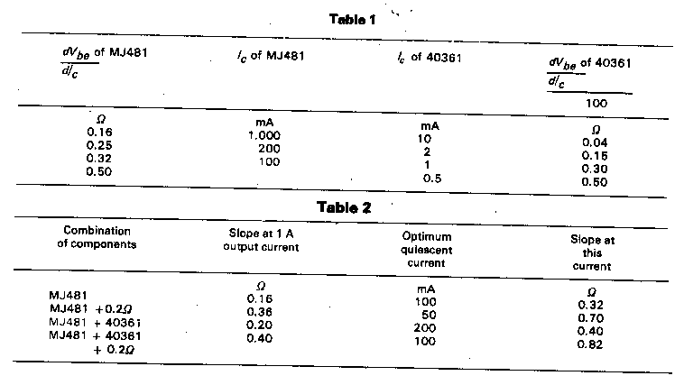
It can seen that the addition of an emitter resistor reduces the optimum quiescent current and of a driver increases it although either addition reduces the overall mutual conductance at all currents. The effect of finite values of R is to reduce the change introduced by the driver.
The p-n-p/n-p-n configuration is more complicated (c.f. Mr. Baxandall's letter in the September 1969 issue), but in general it has a higher mutual conductance (Fig. 2, r=0) than the simple output transistor. With common values of r the combination is linear down to much lower collector currents in the output transistor, giving a lower half-slope current. With a high source impedance the optimum quiescent current for a complementary or quasi-complementary output stage is not so readily defined. It may well be Mr. Linsley Hood's experiences in these circumstances which leads him to the conclusion (August issue) that the optimum quiescent current varies inversely with the absolute magnitude of the current gain in half of the output stage.
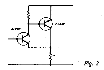
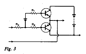
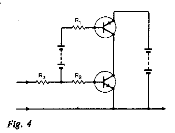
The circumstances which would exist in a practical design" are precisely those put there by the designer; source impedances of under 1 ohm are perfectly feasible. It begs the question to insert resistors in the base lead before even measuring the basic properties of the transistors. The mutual characteristic so obtained is only relevant to a complete amplifier which has these impedances in series with each half of the output stage - resistors R1 & R2 in Figs. 3 & 4 - excepting pure class B using transistors which cut off perfectly and do so with zero base-emitter voltage. If R1 & R2 are zero, and R3 is finite, the overall transfer characteristic of the complete output stage is best not looked at in terms of the mutual conductance measured when one transistor is omitted.
I apologise for making objections in terms of the article, since it does not convey the sense that the author intended, but I based my arguments on the design itself. The source impedance to the output stage is genuinely low. The minimum current gain of an MJE521 at 50 mA collector current is about 80, giving a drive impedance of 70 ohm at the most (derived from the 6.8 kohm resistor). The input impedance of the output stage varies between 50 and 100 ohms in the 15 ohm version with output transistors of current gain 100. It is the inappropriate ratio between these two quantities which is responsible for the effects to which I referred.
It would be convenient if the bootstrap capacitor could supply the extra current required to drive low gain MJ491s which need a base current in excess of the standing current in the driver stage. This could only occur if the bootstrap capacitor temporarily sustained a greater voltage than it does under static conditions. This situation arises during a short negative transient (MJ491 on) a short time after a long positive excursion (MJ481 on). Short and long are referred to the time constant of the bootstrap capacitor and R4 in Fig. 3 of the article. Quite how common these conditions are in music (with whatever d.c. components there might have been removed well before bootstrap capacitor has its say) I can't imagine.
The other points I should like to make are best left to a future date - we both appear to be drawing on material which should see the light of day in articles rather than in letters.
DUNCAN MITCHELL,
Postgraduate School of Electrical and Electronic Engineering,
University of Bradford.
HISTORY: Page created 20/07/2001
12/01/2002 December 1970 letter added