The Class-A Amplifier Site
This page was last updated on 17 May 2001
The Capacitance Multiplier
The power supply for the original 1969 JLH design included a form of capacitance multiplier to reduce the amount of voltage ripple on the supply rail. The capacitance multiplier circuit has been developed further, by Rod Elliott of Elliot Sound Products, and the results published as Project 15 at the ESP Audio Pages. The modified circuit is suitable for both the original 1969 JLH amplifier (using only the positive half of the circuit) and the 1996 update. The design considerations for the capacitance multiplier, its benefits, and a comparison with voltage regulators are included in the Project article. I do not propose to repeat the information here, but have included a copy of the final circuit schematic for information (Figure 1.).
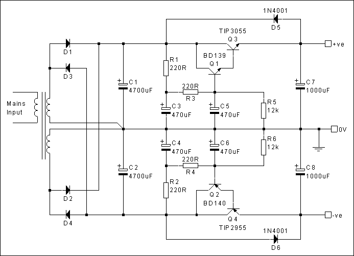
Figure 1. The final circuit (courtesy of Rod Elliott and The ESP Audio Pages)
If desired, this circuit can be modified slightly to use the same type of pass transistor in both the positive and negative supply rails. This will allow the same transistors to be used as those in the output stage of the amplifier, which could result in some cost saving by buying a quantity of the same type of device. A greater advantage results from the opportunity to match the gain of the amplifier output transistors. Matching the gain gives the minimum harmonic distortion for this amplifier and, after selecting suitable pairs for the amplifiers, the rejected transistors can be used in the capacitance multiplier(s). The modified circuit is shown in Figure 2. VR1 and VR2 are adjusted to give equal (but opposite) voltages on the supply rails and to give the required volt drop across the pass transistors of approximately 3V.
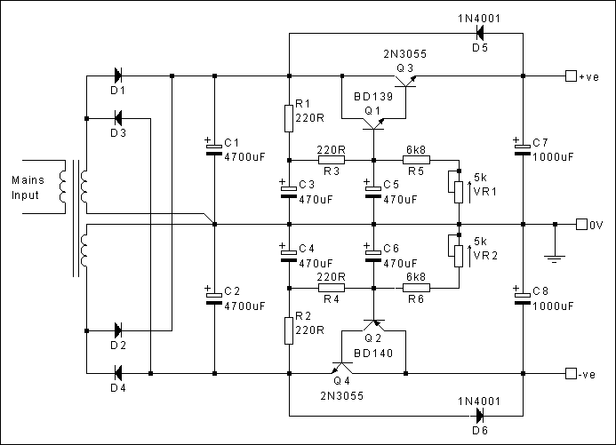
Figure 2. The revised circuit which allows both pass transistors to be of the same type.
The required size for the main smoothing capacitors (C1 & C2) depends upon the load current. I suggest that the minimum capacitance should be as shown the following table. The preferred value for the capacitors is also given (this is approximately 1.5 times the minimum).
|
Quiescent Current (A) |
Peak Load Current (A) |
Minimum Capacitance (uF) |
Preferred Capacitance (uF) |
|
1 |
1.5 |
4,700 |
6,800 |
|
2 |
3 |
6,800 |
10,000 |
|
3 |
4.5 |
8,200 |
12,000 |
|
4 |
6 |
10,000 |
15,000 |
Please note that these figures have been revised since the original publication of this page and reflect more recent (and accurate) simulations I have changed my simulator program and models to ones that give more realistic results.
A simple capacitance multiplier circuit is shown in Figure 3. This gives the easiest possible physical construction (i.e. the fewest components). The performance of this simple circuit in terms of ripple voltage reduction is not as good as the previous circuits, but it is still more than adequate to reduce any hum to inaudible levels (unless you have extremely sensitive speakers).
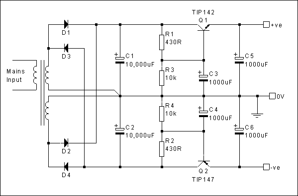
Figure 3. A simple capacitance multiplier
Again, the required size for the main smoothing capacitors (C1 & C2) depends upon the load current. It is generally greater than that for the previous circuits. The following table gives the minimum and preferred values.
|
Quiescent Current (A) |
Peak Load Current (A) |
Minimum Capacitance (uF) |
Preferred Capacitance (uF) |
|
1 |
1.5 |
4,700 |
6,800 |
|
2 |
3 |
6,800 |
10,000 |
|
3 |
4.5 |
10,000 |
15,000 |
|
4 |
6 |
15,000 |
22,000 |
In the two previous tables, the 1A and 2A figures are relevant to a single 1969 or 1996 version of the JLH amplifier. The 3A and 4A figures are appropriate for a pair of each amplifier version operating from a single power supply.
HISTORY: Page created 01/05/2001
16/05/2001 Diagrams amended to correct polarity of D6. Simple capacitance multiplier circuit added
17/05/2001 Recommended capacitor sizes updated. Minor text changes