The Class-A Amplifier Site
This page was last updated on 27 November 2002
Design Notes
Design notes for the JLH Class-A amplifier.
The 1996 version using the specified transistors with +/-22V supply rails and a quiescent current of 2A has an approximate rms power output, into a resistive load, of 10W into 16ohm, 20W into 8ohm, 15W into 4ohm and 10W into 2ohm.
For minimum distortion, Tr1 and Tr2 should be a matched pair. If this is not possible, the device with the higher gain should be used in the Tr1 position.
Low gain output devices such as the 2N3055 should only be used with a high gain driver transistor, for example the 2N1711 or 2N3019 (or a suitable alternative - perhaps a specially selected BD139).
The output transistors should ideally have an fT of 4MHz or more, though many amplifiers have been successfully used with 3MHz devices (or even lower). For information, the 2N3055 datasheet from ON-Semi quotes an fT of 2.5MHz and that from ST, 3MHz (though other 2N3055 manufacturers quote a figure of 0.8MHz). TIP power devices are usually 3MHz.
Because of the high dissipation in the output devices (about 45W each for the 1996 version), I suggest that any proposed output transistor should have a thermal resistance (junction to case) of less than 1°C/W. Alternatively, a parallel pair arrangement (with 0R1 emitter resistors) can be used. For guidance on heatsink sizing and transistor mounting see the ‘Heatsinks’ article at the ESP Audio Pages.
To minimise quiescent current and dc offset drift due to temperature rise, resistor R10 (0R33) should be a 7W or 10W type or 3 x 1R0 3W in parallel. The resistor(s) should be stood-off the pcb to ensure adequate ventilation. For the same reason, Tr5 should have an adequate heatsink. From experience, I would suggest a minimum of 10 °C/W, though around 6°C/W would probably be better. If a BD140 is used instead of the MJE371, a larger heatsink will be required since its thermal resistance (junction to case) is much higher than that for the MJE371. When laying out the pcb, try to keep R10 and Tr5 away from the output transistor heatsinks.
I must stress that the circuit diagram (Figure 3.) in the original article for the 1996 version contains an error. The negative end of the feedback capacitor (C4) is shown connected to the –ve supply rail. This will result in excessive hum due to the supply rail ripple voltage being injected into the feedback path (Tr4 emitter). To prevent this problem, the negative end of C4 should be connected to the 0V (earth) point.
The value of the input capacitor (C4 or C1) can be usefully increased to lower the low frequency –3dB point and improve the bass response of the amplifier. I suggest a value of between 1uF and 2.2uF. A polypropylene capacitor is preferred in this position.
The value of the blocking capacitor in the feedback circuit (C3 or C4) can be usefully increased to reduce the low frequency distortion of the amplifier. Values between 470uF and 1000uF would be suitable. Rudy van Stratum has tried values up to 1000uF and has found that 470uF sounded best in his modified (dual rail) 1969 version.
In theory, and in simulation, increasing the value of the bootstrap capacitor (C1) in the 1969 version to between 470uF and 1000uF reduces the frequency at which low frequency distortion starts to increase due to the non-linearity of the current source that controls the output stage quiescent current. Rudy has also tried values up to 1000uF in this position. Contrary to expectations, 1000uF caused a ‘thickening’ in the bass and a loss of ‘air’ and ‘finesse’ in the treble. He has now found that 470uF gives the best results.
I previously suggested by-passing all electrolytic capacitors with a 100nF polypropylene capacitor (in parallel with the electrolytic). This may not have an audible effect, but it ensures a low esr at high frequencies. Rudy has reported that, when he has tried paralleling capacitors in the past, the sound quality has deteriorated in comparison to a single capacitor. His exact comments were:
“About 10 years ago this was standard practice for me, everywhere I used a small film cap to better the high frequency behaviour. But I believe now that a good design does not need such things, the best amplifiers I heard use no such things. And on more than one occasion this bypassing produced sharp edges to the sound. Somehow it seems that you can hear two different capacitors. Compare it to the difference between a good broadband (full-range) speaker vis-a-vis a two-way system: you always hear two units. Some of the natural integration is gone.”
As other articles I’ve read appear to come to the opposite conclusion, I’ll keep an open mind on this issue.
I have received two reports recently regarding a problem with oscillation of the 7815 voltage regulator in the 1996 design. There are several cures for this problem. One would be to replace the 7815 (and C3, RV1 and R1) with an adjustable constant current source (a decoupled resistance, an FET, an LED/transistor or a two transistor circuit). The current source will need an adjustable output of between 0.4 and 0.5mA. The second solution is to improve the stability of the 7815 by increasing the output capacitor (C3) to between 22uF and 100uF. In addition, it could be worthwhile adding a resistor from the output of the 7815 to earth to ensure a minimum output current. A value between 3k and 4k7 should be suitable. None of the 7815 data sheets that I have been able to find has specified a minimum output current, but adjustable regulators such as the LM317 call for a minimum current of around 3.5mA. From one constructor’s experience, the 78L15 seems to be more prone to oscillation than the standard 7815 so, even though the current draw is less than 0.5mA (or 1mA if one regulator is used to feed both channels as in the original diagram), I suggest using the latter.
When using the original (1969) bootstrap arrangement for quiescent current control, care must be taken to ensure that R1/R2 (1969 article Fig. 3) or R1/RV1 (1996 article Fig. 1) are adequately rated. The current through these components is slightly greater than the sum of the output transistor base currents. The output transistor base current is the output stage quiescent current (Iq) divided by the current gain (Hfe) of the output devices. The current through R1/R2 or R1/RV1 is therefore approximately equal to 2 x Iq / Hfe.
If the current/resistor values of Table 1 (1969 article) and output transistors with a current gain of 100 or more are used, the resistor power ratings shown in Fig 3 (1969 article) are adequate. If low gain (circa 50) output devices are fitted, the resistor power ratings should be increased to about double those shown in Fig 3. For other resistor values or quiescent currents, the required power rating of R1/R2 or R1/RV1 should be calculated.
Whilst it should not be difficult to obtain fixed resistors with the required power rating, a preset potentiometer could be more of a problem since the more common ones are only rated at 0.5W or 1W, though higher rated devices are available. It must be remembered that the power rating of a preset, when used as a rheostat, is proportional to the length of track in use. It is therefore necessary to determine the power rating from the current flowing through the preset and its total resistance value. It may be necessary to use a fixed resistor in series with a lower value preset to form RV1 in order to keep within the power limits of the preset.
For those who prefer the greater simplicity of the 1969 version, but wish to avoid the output capacitor (C2), the circuit can be modified to operate off dual supply rails. Figures 1 and 2 illustrate two methods of achieving this. It must be stressed that Option 1 has yet to be verified in practice (so far as I am aware), but Option 2 has been successfully implemented by at least one constructor.
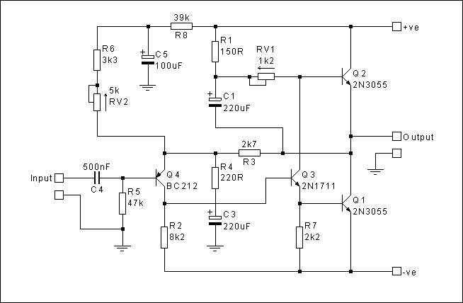
Figure 1. 1969 design with dual supply rails (Option 1)
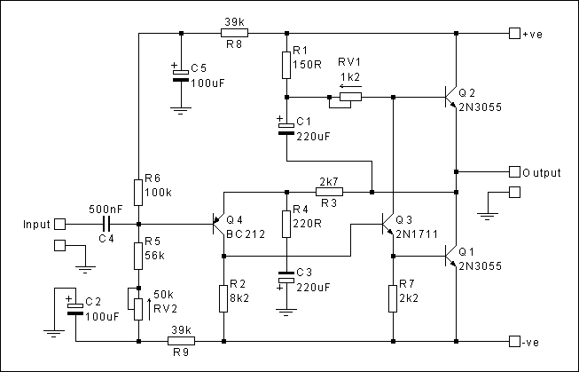
Figure 2. 1969 design with dual supply rails (Option 2)
For more design information relevant to this type of amplifier, see Project 36 at the ESP Audio Pages. The amplifier in this project is very similar to the JLH 1969 version (the main difference being the addition of a transistor to the quiescent current control circuitry) and Rod Elliott gives a good explanation of how he determined that this is the optimum topology for a simple solid-state Class-A amplifier.
HISTORY: Page created 01/05/2001
10/05/2001 Added link to Quiescent Current and DC Offset page
16/05/2001 Diagrams redrawn
05/06/2001 Polarity of C3 in Figure 2 corrected
05/08/2001 Capacitor notes revised and 7815 oscillation notes added
31/01/2002 1969 bootstrap resistor power rating notes added
27/11/2002 dc offset servo paragraphs removed