The Class-A Amplifier Site
This page was last updated on 20 July 2001
[ Back to Index ]
JLH Headphone Amplifiers
The following two JLH headphone amplifier circuits have been included because of their relevance to other designs on this site.
The first circuit was originally published in Hi-Fi News and Record Review in January 1979. It is, in effect, a JLH Class-A amplifier modified to suit a higher impedance load. I do not have a full copy of the original article but have listed, after the schematic, some information on the performance of this design. The oscilloscope traces included in the article showed an identical 10kHz square wave performance into 100ohm, 100ohm/0.22uF and headphone loads and pure second harmonic distortion with a 1kHz and 10kHz sine wave input.
The second design was first published in ETI in the mid 1980s (the copy I have is from Electronics Digest, Winter 1985/86) and was part of a series of articles relating to a complete integrated amplifier. The circuit bears more than a passing resemblance to the Hiraga Class-A designs. The full text from the original article is reproduced below the schematic.
Circuit 1
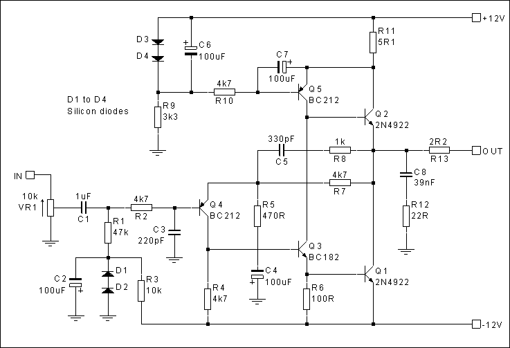
Performance
The aim of this circuit was to take advantage of the design freedom conferred by the relatively low load demands of the normal headphone, and to design a system free from the constraints and compromises inherent in normal power amplifier circuits. It is hoped, therefore, that this will be regarded not as a poor man’s substitute for a power amplifier, but rather as a reference standard against which existing higher power units can be judged.
Performance data
|
Frequency (Hz) |
T.H.D (%) |
|
100 |
0.014 |
|
300 |
0.007 |
|
1k |
0.008 |
|
3k |
0.017 |
|
10k |
0.044 |
THD – exclusively second harmonic (includes noise), measured at 1Vrms across headphones having 100ohms (nominal) impedance.
Turn-off and turn-on time – less than 0.5us.
Settling time (to within 1%) – 6us, not affected by load reactance up to 0.22uF.
Recommended load – minimum 8ohm; ideal 35ohm to infinity.
Circuit 2
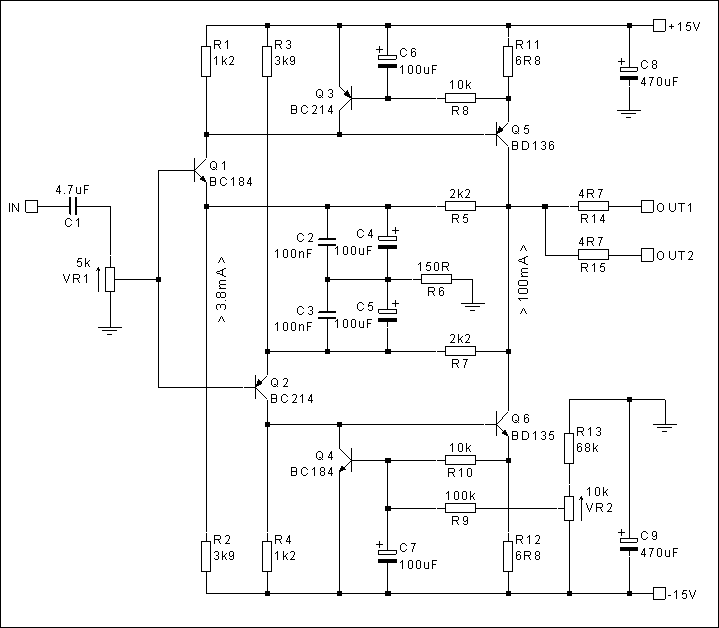
The Headphone Amp
If the preamp is a separate unit from the power amp, it is a very useful thing to have a small headphone amp capable of driving a couple of pairs of phones, within the preamp box. However, if this amplifier is to be an accurate monitor of the signal delivered to the power amp and if, in the sort of architecture proposed for this unit, in many cases the signal from the auxiliary units will be routed directly to the power amplifier, the quality of the headphone amp must, if anything, be higher than that of the power amp itself.
Fortunately, the headphone amp has a much easier job to do, in that neither the output power requirements nor the load characteristics are so severe, since headphones typically have a load impedance of 100-2000ohms, and only require 1-2V max RMS, for normal output. There are of course electrostatics, which may demand 5-10 watts, at loads down to a few ohms, but these are best driven from the power amp anyway, and the ‘8ohm’ headphones will require a very low drive voltage anyway.
Since only a low power output is required, a class-A stage is perfectly feasible. Because only smallish output transistors are needed, 10MHz fT devices are easily found, and, in any case, class-A operation makes the HF response good. The only other thoughts which commend themselves are that the design should be completely symmetrical, and direct coupled to the output, and that where NFB bypass capacitors of electrolytic type are used these should have a polarising voltage across them. It will also help sound quality if the amplifier has few stages, using discrete components, and no slew-rate limiting HF roll-off components are needed.
A design which meets these requirements, and gives an excellent sound quality is shown in the schematic.
The basic amplifier system is as follows. A pair of push-pull input transistors, Q1 and Q2, drive a push-pull pair of output transistors, Q5 and Q6. Negative feedback is taken from the output point to the emitters of Q1 and Q2, and the load connected between the joined collectors of Q5 and Q6. For adequate class A operation the output transistors should pass, say, 100mA each. With a +/-15V supply, this would mean 1.5 watts dissipation, so a smallish heatsink, perhaps 1.5” square, will be needed for each.
If the output transistors have a minimum current gain of 50, then each may require a maximum current input to their bases of 2mA. In order to provide this, with a bit to spare the input transistors, Q1 and Q2 should normally pass about 4mA. If these have a current gain of 150, their base currents will be 0.004/150=26.7uA, which gives an input impedance of about 9k. The input gain control (and since this has to provide a ‘balance’ feature too, this should be the twin concentric spindle type) must therefore be a good bit less than this: a value of 4k7 will be fine. Unfortunately, some of the input signal sources may have too high an impedance to be able to drive this. It may therefore necessary to provide an input buffer (see below), where otherwise a 'straight through' signal path would have been used. (A 3-head recorder system will normally have a 'line' output impedance (600 ohms) so this can drive the headphone amp without problems.)
Returning to the headphone amp circuit, we must now provide a source of emitter current for Q1 and Q2, and a means of controlling the current through Q5 and Q6. The emitter current for Q1/Q2 is derived from the +/-15 volt lines through R2 and R3. For a 14.5V drop and 4mA flow, this would require a resistor value of 3625 ohms. The nearest preferred value is 3k9, which will pass a current of 3.7mA, though some 250uA will also flow through R6 and R8.
Looking now at Q5, (the circuit operation for Q6 is the same), a small resistor (6R8ohms) in its emitter circuit senses the current flow. If this is too high, a forward bias is applied to the DC amplifier transistor Q3, through R8, (C6 removes all audio signals from this point), which will cause Q3 to conduct and steal drive current from Q5 base, holding the collector currents of Q5 (and Q6 for which the operation is identical) to the chosen average value.
Negative feedback is applied from the outputs of Q5 and Q6 to the emitters of Q1 and Q2. This gives a measure of DC output voltage control, but this can be fine-trimmed by R9, R13 and RV2 which operate to adjust the collector current of Q6 relative to Q5. A DC output level of 0V+/-50mV is adequate. Because the bases of Q1/Q2 are joined together, their emitters will sit at –0.55V and +0.55V respectively, which provides a standing 0.55V potential across C2/C3 and C4/C5. C4/C5 should be low ESR aluminium electrolytics bypassed by C2/C3 polypropylene or polycarbonate 100nF types.
On typical headphone load impedances, the output THD is substantially that of the input signal, as is the transient response.
Buffer
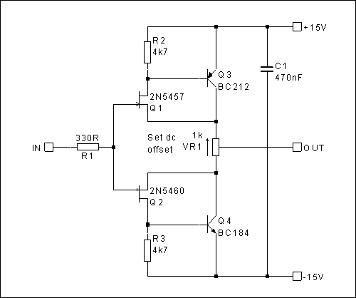
The bipolar-FET symmetrical compound source follower circuit works extremely well, with negligible steady state or transient distortion.
[ Back to Index ]
HISTORY: Page created 20/07/2001