The Class-A Amplifier Site
This page was last updated on 19 July 2001
Please note that when translating this article I tried to keep as close as possible to the original text, though a few changes have had to be made to ensure that the translation makes sense. Whilst reading the article, please bear in mind the following alterative meanings for some of the translated words: batch - type; saturation - onset of clipping; rate of distortion - distortion level; offset - drift; enclosure - speaker.
Construction of a 20W Class A amplifier
3 – The final version
Jean Hiraga – Gérard Chrétien
(l’Audiophile No. 15)
This amplifier has already been the subject of two articles in Issues 10 and 11 of l’Audiophile. In this third part, it will be a question of the practical aspects and the final design, as well as final adjustments and various useful recommendations. Thus, we think that this will make it possible for readers to better understand the circuit, its advantages and its characteristics. Many readers have criticised us for the lack of practical information, which has slowed them down when undertaking a construction of this type. We will also try to give all the small details that it is good to know and which avoid many obstacles.
At the end of this article, it will be a question of the measurements of the final version that have been made in our currently well-equipped laboratory, Editions Fréquencies. We will also mention some criteria for the recognition of the subjective quality of good amplifiers. This is a delicate subject, which will be covered here in such a way that it should not relate to personal appreciation or the taste of the listener, since it keeps to the distinction between true sounds and modified sounds…
Latest developments
In the diagrams described in Issues 10 and 11, some resistance values had been calculated according to the batch of transistors used for the prototype. Everyone knows that the variation in characteristics, particularly the Hfe of transistors, can have an important effect. The transistors used in this design have a number and an alphabetic code placed after the reference. This makes it possible, according to the manufacturer, to determine the limits of the variation. In spite of this, the variations still remain significant and ‘pair matching’ is desirable. On this subject, various comparisons were made on the prototypes using either very “close” pairs or pairs from the same batch. The differences noted by measurement as well as listening were not major. Nevertheless, we considered it preferable to carry out ‘pair matching’. We must say that in the case of a direct coupled amplifier, such as the 50W Kanéda, this kind of problem is infinitely more critical. For this circuit, this “accommodation” constitutes a practical advantage that guarantees optimal operation, even after long use.
As we will mention a little later on, some minor modifications were made to the final version because of the question of the difference between batches of transistors.
Influence of the supply voltage
On the first prototypes, the supply voltage had been adjusted to +/-18V which made it possible to obtain a power of 20W in pure class A in the extreme case of saturation (showing itself by clipping of the sine wave). The batch of transistors used for these prototypes were different, the Hfe of the second stage was less and the Hfe of the output stage was greater. The first four transistors should have, as far as possible, an identical Vbe characteristic for an Ic current of 1mA. The series of transistors used in the kits gave performance measurements identical to those of the prototypes, except however for a faster saturation of the driver stage and the output stage, for the reasons indicated above. Thus, the value of the power supply voltage becomes a paramount factor. In spite of an oversized power supply transformer, 6A whereas consumption should not exceed 3.4A, the load voltage varied according to the models by a volt or two in spite of the similar specifications. Thus in the first models of the final version, with a low mains voltage, the voltage of the power supply, after the 1ohm Pi filter resistor, reached 17V with difficulty. This slightly lower value was enough to make saturation fall to 15.5W. We thus encountered two problems that went in the same direction: a different batch of transistors on the one hand and a lower supply voltage on the other. In this connection, many Japanese buy American amplifiers and make the error of using them on the Japanese 100V mains, whereas these items of equipment are designed for 117V. This variation represents a considerable loss of power and affects performance in proportions that are far from being negligible: “circuit limiting devices, Zener diodes, power supply regulation….”
As we have mentioned previously, it is necessary that the amplifier works in pure class A in temperature conditions which remain reasonable, so as to avoid any thermal runaway, loss of quality in prolonged listening and slow deterioration of the power transistors after several years of work (frequently the case for a class A amplifier pushed too much). This project also avoids all useless complications of the circuit. The power transistors 2SA627 and 2SD188 are very current transistors in Japan and they are very appreciated for their subjective qualities. They have a Pc of 63 W. However, it is important to find the best compromise for reliability / maximum output power.
The maximum power is determined by the formula:
Pmax = (2 Vcc x CLoss)^2
8 RL
Vcc is the voltage applied to the transistor, RL the impedance of the load (normally 8 ohm) and CLoss "collector loss", the resistance loss of the collector, which is about 0.8 to 0.85 for the series used.
This gives for a Vcc of 18V a Po max. of:
Po max. = (2 x 18 x 0.85)^2 = 14.63 Watts
8 x 8
In fact, good adjustment of the different components makes it possible to slightly exceed this theoretical limit of saturation by 1 to 2W.
Although it is possible, after modification, to reach the level of saturation at more than 20 W, it is essential to take account of two very significant points:
- never to exceed the quiescent current of 1A per transistor. For this current of 1A, the collector dissipation is 24 W, that is to say 1/3 of the max. collector dissipation (63 W).
- not to exceed a Vcc of 24 V, the practical limit of the design, which will then require heatsinks of greater dimensions and a good ventilation. In this borderline case, the power changes to:
Po max. = (2 x 24 x 0.85)^2 = 26.01 Watts,
8 x 8
which could even possibly allow one, by adjusting some resistances at the time of measurement, to reach nearly 28 W.
However, the modification was not made with an aim of pushing the circuit to its practical limits, but to make it work in full safety, which can never be repeated enough. Thus, even after many operating hours, the heatsinks do not exceed 70 degC, under average conditions of ventilation.
Consequently, the voltage Vcc selected after modification must be between 19 and 21V (dc voltage applied to the circuit), which approximately gives a saturation value of about 20 W.
The two modifications produced
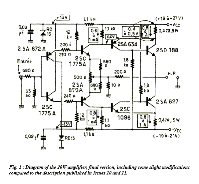
Perfect complementary pairs, which implies all parameters together and not just the precise condition of equivalence of Hfe at one current, do not exist in practice. We have already indicated this difference between PNP and NPN previously, a difference which had led us to slightly unsymmetrical values of resistance between the first and the second stages. In the first diagram, the values were respectively 200 and 300 ohm. In the final version, they change after adjustment to the more precise 200 (210 ohm) and 240 ohm. Saturation is thus quite symmetrical.
For the second stage, which must provide 8V across its 1.1 kohm load for the base of the output, the value of Vbe was readjusted by putting two 680 ohm resistors in parallel with the 500 ohm trimmer. As indicated in the preceding articles, the 12 kohm resistor adjusts the gain and the quiescent current of the output stages. It is not recommended that this value be altered.
Let us mention for the readers eager to remake these adjustments, that it is advisable to take account of the symmetrical circuit. The direct connections can make various adjustments interfere, one with the other. In particular, the 200 and 240 ohm resistors, optimised at the time of the adjustment of the symmetry of saturation, cannot be adjusted individually, but must be altered simultaneously. This can be carried out using two temporary trimmers, which will be then replaced by fixed resistors. It should be noted that this adjustment is significant only at the limit of saturation. Below this limit, no difference is audible, even by preserving the original values of 200 to 300 ohm. We however preferred this finer development because it allows an improvement in the value of distortion, with an unchanged power supply voltage, and thus more reliable conditions of operation. It goes without saying that the adjustment of the trimmer cancelling the output voltage residual remains indispensable in spite of this modification.
Negative feedback and dc offset
The value of the 200 ohm resistor, which connects the output to the wiper of the trimmer, should not be modified. If the amplifier is to be pushed to its power limits, that is to say a voltage of +/- 24 V, one can reduce the value of this resistor to 150 ohm, which results in a slight increase in bandwidth and a reduction of the rate of distortion.
The aim of the negative feedback, its rate being about fifteen dB, is mainly to minimize the risk of dc offset at output. This offset remains very acceptable, note that it exists in all direct coupled amplifiers, as is the case of the present circuit. It remains below 100mV when tantalum resistors are used, along with the 500 ohm trimmer, reference Cosmos RA12P. The latter is the only one to still have an affordable price and it is characterized by low noise and a very low thermal drift, at best under 30 PPM/degC. The better trimmers rarely have values lower than 100 PPM/degC. This trimmer can be replaced by a model of the same type, but with a value of 50 ohm and with two 150 ohm resistors in series. This gives an identical value, within a few ohms close to the equivalent value obtained with a 500 ohm trimmer and two 680 ohm resistors in parallel, which is approximately 180 ohm for each half of the trimmer. Although the adjustment with the 500 ohm trimmer is very simple, it is made without a signal on the preferred input and with the outputs not connected to the enclosures, the 50 ohm trimmer has the advantage of giving a wider range of adjustment.
Current in the second stage
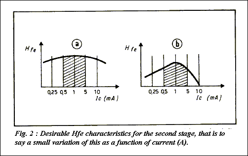
The current in the transistors of the second stage must about 0.8 to 1mA as indicated on the diagram of figure 1. This current is related to the value of Hfe of the transistors. It is the variation of this value between the various batches of transistors which led us to the minor modifications of resistance described previously. In reality it is not the value of Hfe itself which is most significant but rather the variation of this parameter as a function of the collector current. In figure 2 are shown two types of complementary pairs. In A we have a good pair in which the Hfe varies little as a function of the current. In B the variation is much more severe, it is a less desirable pair. It is a point that is thus important and that was advisable to announce.
Quiescent current
The output stage did not undergo any modification. One can measure the quiescent current by measuring the voltage across the 0.47 ohm resistors, this must be set depending on the value of Vcc and the desired power to between 0.8 and 1A. The 1.8 kohm bias resistors can be increased slightly by a few hundred ohms when the voltage is increased, with a maximum value of 2.4 kohm for a +/- 24V power supply.
Power supply considerations
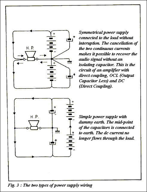
The power supply being symmetrical as well as the circuit, a small imbalance brings a noticeable difference in consumption on the two +/- power supply branches. In normal functioning, this consumption must be identical for the two branches and brings, for an equivalent current, the cancellation of the dc residual at the output. The wiring diagrams in figure 3 explain the process. It is completely similar to that of valve amplifiers without output transformers and with symmetrical power supplies. When the dc residual is cancelled at the output, this corresponds with the minimum rate of distortion. It is related to the ‘pair matching’ of the output transistors.
In connection with the dual power supply, it should be noted that the negative pole of the load is connected to the mid-point of the power supply secondary. In this case, it effectively acts as two distinct power supplies, where the equal currents of opposite direction are cancelled in the load, at the terminals of which nothing more than the amplified signal will be found. However, it is possible, as it is in the case of O.T.L type valve circuits with a single power supply, to remove the mid-point of the transformer secondary. The negative pole of the load is thus connected to a dummy earth. The time-constant of the power supply capacitors being significant, a slight adjustment of the trimmer can bring a momentary offset, which will return little by little to zero. This circuit has the advantage of better protecting the loudspeaker, but has the disadvantage of a single current value in the power stages, even if in the case of a symmetrical power supply one part of the push-pull stage outputs more than the other. It should be also said that the earth point is floating in the case of such a configuration. However, the time-constant being extremely low, the difference is not audible. On the other hand, the fact that one can indirectly consider the load as being in series with the power supply can have audible consequences, which would tend to prove that the quality of the capacitors used in such a type of power supply would have a subjective influence more marked than in the case of a symmetrical power supply. However, the two configurations are interesting, each one having advantages and defects; but everything depends upon the application.
Offset problems
For our present circuit, the power supply is of symmetric type. One never should lose sight of the fact that an amplifier with direct coupling from the input to the output amplifies the dc current without attenuation. Of course, this aspect represents an unquestionable advantage in traditional circuits, by the fact that no coupling capacitor is inserted in the signal path. Thus, the colourations brought about by these capacitors are eliminated, the phase response is much more linear and the transient response is improved (refer to the oscillograms). However, this direct coupling can be a big danger for the loudspeaker, when the link preceding the amplifier, the preamplifier in fact, is affected by a slight dc offset at its output.
Badly adjusted, the Kanéda preamplifier can present this danger, if the 0.4 uF capacitor is not inserted at output of the RlAA stage, before the volume potentiometer. The linear section, because of the low gain of the stages, does not pose this problem. The input stage, itself, has a very high gain and the negative feedback is dc connected to the input. Moreover, the similar form of the RIAA correction amplifies the offset if it is present. Thus, indeed after meticulous adjustment, this offset can fall to below 50 mV, even 10 mV. This offset in itself is not critical. However, an instability in the power supply, the disconnection of the input phono, can be enough to cause an offset of a few hundreds of mV.
The amateurs who prefer to connect RIAA stages to the input of the amplifier, without using the linear stage, will have to pay great attention to this point. It is clearly understood that it is preferable to use the minimum of electronic stages, the risks of degradation of the signal can only be less for it. In this case, the 0.4 uF coupling capacitor will have to be selected carefully. Naturally, high quality silver plated mica capacitors give excellent results. However, the prices are extremely high, between 300 and 500 F each. We recently found an excellent compromise with a 0.47 uF ITT PMT series 250V capacitor (and not 400 or 630V) partially coated with " super black ", the process eliminating the electrostatic type leakage of these passive components
Power supply of the final version
The photographs of figure 4 show the final appearance of the amplifier. It looks like a rather flat and square chassis, on which is seated an openwork cover with three sides. The heatsinks are laid out in line on the back face, and the lower part of the chassis is latticed under the heatsinks, so as to create a chimney effect to allow a good release of emitted heat. The printed circuits are laid out flat on the chassis, in a symmetrical way, that is to say the inputs are placed towards the centre to shorten the wiring.
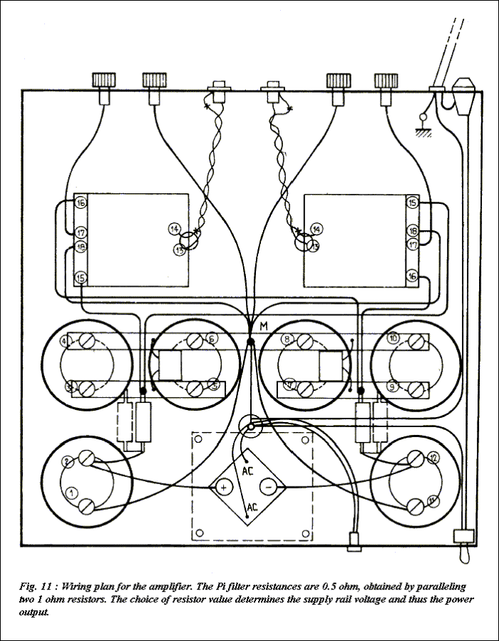
The power supply occupies more than half of the volume. It comprises six large 60 000 uF, 25V, capacitors, a total of 360 000 uF. The diode bridge, imposing due to its size, sits under the transformer. It is important that this has large dimensions because of the load current with high crests. The Pi filter uses a resistor of 1 ohm or 0.5 ohm depending on the desired value of Vcc. Thus, for each half of the symmetrical power supply, one finds successively after the diode bridge, a 60 000 uF filter capacitor at the input, followed by the filter resistor, which is connected to the two output capacitors of 60 000 uF each.
A point must be made concerning the filter resistors. These are an inductive type wound on laminated steatite and with a 15W power. In normal operation, these resistances work at a fairly high temperature that remains nevertheless below the limits of maximum dissipation, since the real dissipation is around 12W. It is appropriate, when first applying power to the equipment, to place the wiper of the 500 ohm trimmer on the printed circuit at mid-track. In this position, the dc residual at the output is practically zero, whereas at the end of the track consumption in one half of the power supply can become greater and exceed the normal value, which results in abnormal heating of filter resistor.
Figures 4(a), 4(b), 4(c) and 5 can be viewed here.
The earth wiring
This is a very significant point about the construction. Indeed, when one uses unregulated power supplies with large filter capacitors, the harmonics of the mains can "cross" this filtering without being attenuated. This is characterized, not by a whirr, but by a characteristic "bzzzz". It comes from the ac residual of the filtering, in which the switching peaks of the silicon diodes are included. These peaks can be seen on the oscilloscope and their height can be reduced by placing small capacitors, whose value can be adjusted from 10 to 20 nF, in parallel with the diodes of the bridge. However, even in the absence of these capacitors intended to absorb the peaks, it is possible to completely eliminate the residual background noise from the power supply and to make it fall below the noise level of the amplifier, which is already at a very low level in the present case.
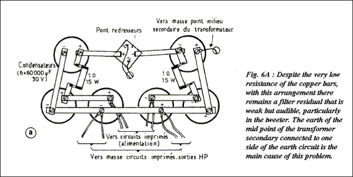
For this, it is necessary to follow the star earth wiring, that is to say to connect the various earths at a single point. Figure 5 shows an example of the power supply wiring. The common earth consists of a copper bar. In spite of the thickness of this, and thus a negligible resistance, we encountered problems whose cause came from a lack of symmetry of the earth point.
Figure 6 shows the two types of wiring: in A, the power supply displays the defect evoked above; in B, a power supply with a single earth point and star earthing. The solution B is that which gives the best results, it must be used for the power supply wiring of the amplifier.
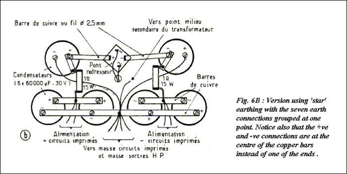
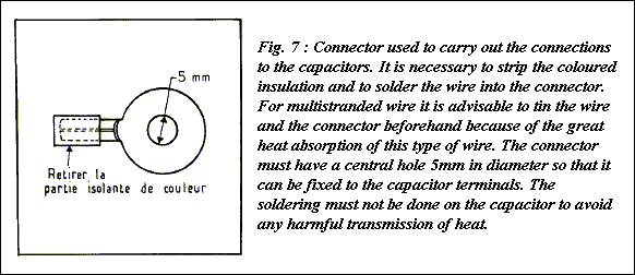
To connect the capacitors, the most practical solution consists of using copper bars 1.5 to 2mm thick mm and approximately 15 mm wide. One can also use copper braid of an equivalent width. For fixing the connections, one can directly solder onto the bars or the braid, or use connectors (fig.7) for which one removes the insulation to solder the wire, which is normally held tight with a special grip. In the case of soldering to the bars, one can perforate these as a preliminary with approximately 1.5mm diameter holes, which facilitates the soldering operation. It is also important to unscrew the capacitors before soldering so that they do not absorb heat dangerously. The soldering iron must have a sufficient power, from 80 to 100W, so that the solder joints are clean and easily carried out, taking into account the thermal inertia. As soon as the solder cools, one can immediately (before the bar cools) pass a soft rag over the solder joints to remove the surplus resin. Then it is necessary to take care to screw up all the plates on the capacitors. For wiring, preferably use multi-stranded wire of the Lify type, of 1mm2 or 2.5mm2 cross-section. Note that 2.5mm2 wire is more delicate because this, wire which contains more than 1 000 strands, absorbs heat and solder very well. It is thus necessary to take the time to well tin the wire twice. The first time to make the solder penetrate into all the strands. The second time with more solder, but in a shorter time, so that it coats the wire well without penetrating through the strands. With cutting pliers one gets rid of the excess length of the tinned wire. And it is only after having pre-tinned the part to be soldered, bars or copper braids, that one carries out the final soldering operation which will require moreover only very little solder. Thus, one carries out good solder joints without heating the parts too much.
A last point concerning the power supply wiring. The 2.2 uF ITT PMT or PMC type capacitors are mounted on the output filter (2 x 60 000 uF). Let us recall that it is advised to use them because the better high value electrolytics become inductive from 10 or 15kHz, sometimes even from 5 kHz. Also, it is very important to decouple them at the high frequencies. The ITT capacitor is advised for its non-inductive construction, the great rigidity of its reinforcements and its very affordable price. The Lify type wire brings only very little series obstructing inductive effect which could cause a parasitic resonance at high frequency by coil/capacitance agreement, because of its very short length.
One can, of course, fix the two 2.2 uF capacitors directly to the printed circuit. In this case, one can locate them between the power supply +/- connection terminals and the earth of the printed circuit.
The circuit wiring
The circuit of the kit is provided pre-cabled. The power transistors are already fixed to the heatsinks and are connected to the printed circuit, so as to avoid errors of assembly, in particular, the connections of the transistors.
Construction being completely symmetrical, wiring is simple. It is enough to connect the inputs of the Cinch sockets, whose earth is directly connected to the chassis, to the printed circuit using two colour twisted Lify wire. Then, to connect the power supply + and - on each board, as well as the earths taken to the common point. Lastly, to connect the loudspeaker outputs, the red terminal to the printed circuit, the black terminal to the earth point, for the two channels.
The transformer
The transformer which was retained after various tests is a model of excellent quality, impregnated under vacuum and using double C cores. The advantage of the double C core is low radiation combined with a good output and, for equal power, a size that is less than that of a conventional model with laminated sheets. Nevertheless, in spite of an imposing aspect, this kind of transformer is rather fragile, in particular with regard to the size of the air-gaps, that is to say the four flat faces where the C cores come to meet one against the other. The contact must be perfect. A shock or a bad fixing is enough to slightly move the cores and thus widen the air-gap, which is accompanied by a slight parasitic vibration that can be audible. It is necessary in this case to re-examine the fastener of the core tightening tapes or the tightening of the sheets. Perfectionists can mount it on small isolating blocks made out of rubber. In power amplifiers, the parasitic vibration of the transformer is a rather frequent problem. However, this problem of mechanical vibration can always be solved, unless the sheets and windings are badly impregnated. The impregnation under vacuum, which remains the best means of avoiding this nuisance, is not, as one would think it, widespread. On the one hand, for questions of cost price, and on the other hand, for reasons of safety requirements, the prohibiting, in certain countries, of hydrogen for the impregnation operation.
The model selected is pasted with araldite to further limit the risks of parasitic vibrations. It is largely dimensioned, 6A whereas average consumption does not exceed 3A, so that it does not heat excessively, even after several hours of use, 40 degC approximately.
It is advisable, for reasons of accessibility, to solder the wire coming onto the transformer before the mechanical mounting of it.
This transformer has three tapings on its primary, 210, 220 and 240V, to adapt to the mains voltage, but as we saw previously, this has a great influence on the value of Vcc and thus on that of the output power. One can, if one wishes a little more power, use the 210V tapping, even if the mains supply is 220 or 230V. One thus gains 1.2 to 1.5V on the power supply voltage.
The 220V neon indicator lamp has a resistor incorporated, so that it is enough to connect it to the 0 and 220V ends of power supply transformer primary.
Measurements
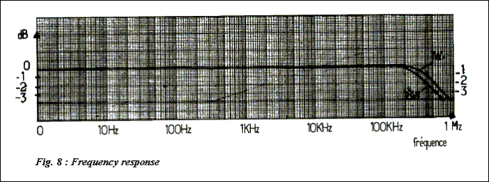
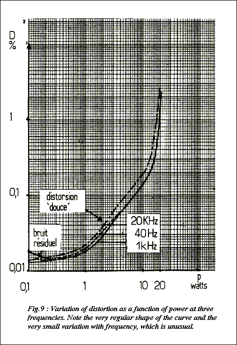
Figures 8, 9 and 10 show the results of measurements. These are rather astonishing when compared to the simplicity of the design. Note however, as we have announced many times, that a search was not made with the intention of reducing the rate of distortion to negligible values; values which, in our opinion, are not very significant when they are located below a certain threshold. The reduction of this parameter is obtained, except for very rare exceptions such as the case of using MOS-FET, VMOS-FET or RET transistors, by the use of one or more negative feedback loops. These, on the other hand, are likely to make the design unstable on a complex load. In this case, without any contrivance, while using conventional bipolar output transistors, the bandwidth extends to -3dB at nearly 1 MHz.
The response to a square wave signal shows the excellent behaviour of the amplifier over all the frequency band. At 20kHz on a capacitive load, 2.2 uF in parallel with 8 ohm, the results are remarkable. They show the excellent stability of the design, since no overshoot is visible on the oscillogram. On a complex load at 40Hz and 20kHz, the results are just as satisfactory. The amplifier is perfectly stable in all circumstances, with an extremely broad bandwidth which give it a rise time of 0.6 uS.
Figures 10(a) to 10(h) can be viewed here.
An interesting point of the design is the characteristic of the power variation as a function of the load impedance. In the majority of the transistorised amplifiers, the power increases when the impedance decreases, to arrive at saturation towards 1 or 2 ohm, at the place where the circuit starts to labour in function. The 20W amplifier, in particular its output stage, has a linear curve, not downward when the impedance goes up, but rounded and rising after 8 ohm to only go down again very slowly for higher values of impedance.
Thus good results were obtained with electrostatic loudspeakers put in parallel or series (that is to say 8 or 30 ohm), without difficulty and without much loss of power or subjective qualities. In addition, on high output enclosures, such as Altec, Onken-Mahul and JBL, the ????? enclosure (l’enceinte accordée) causes a large increase in impedance.
On the Onken bass enclosure, the impedance goes up to nearly 70 ohm, between 15Hz and 50Hz. It is precisely in these regions that the amplifier must best control the loudspeaker. This explains the ability of the 20W amplifier described here, to “hold" the bass region of the Onken enclosure, in spite of a fairly poor damping factor.
As for the rates of distortion, one can never repeat enough that the subjective rate of distortion is much more significant than that measured, and that on this level the smallest things come to influence or modify (slightly or more clearly) the perceived sound. It is true that in certain conditions, it is possible to make several quality amplifiers "sound similar", but it is just as true to say that under other conditions (moreover completely "normal"), it is possible to make these same amplifiers "sound" in a very different way. Generally, the refusal of some to acknowledge hearing a difference between good amplifiers comes from a quality of totally poor listening (which can easily miss the ordinary defects of colouration, or linearity), due mainly to the loudspeakers used, where it is rather difficult to think that 99% of the energy is lost in friction and heat. Like there was always a question since the first issues of l’Audiophile, it is not a question of being for or against the subjective or the objective, of wanting too much to be "Audiophile" (a term taken in a distorted direction, by scandalmongers). The goal is to prove that in subjective listening, there are the facts, the very clear differences of quality, definition, tone, depth of sound, sound balance, at levels certainly more marked than those to which musicians adhere where pianists work several years continuously to make a "note" stand out and where the "bad audiophile" would see neither any progress there nor any difference. These differences, which can appear "too subtle" with the eyes of an engineer believing only in Ohm’s law, are thus certainly not well below the requirements of a musician or a conductor.
HISTORY: Page created 05/07/2001
10/07/2001 Page re-titled and revised
12/07/2001 All Figures added
14/07/2001 Text added
16/07/2001 Minor corrections to text
19/07/2001 Link to Figures 4 and 5 added. Figure 10 moved to separate page.